| CPC G11C 11/4087 (2013.01) [G11C 11/4074 (2013.01); G11C 11/4076 (2013.01); G11C 11/4085 (2013.01); G11C 11/4094 (2013.01); G11C 11/4096 (2013.01)] | 19 Claims |
|
1. A semiconductor memory device, comprising:
a memory cell array including memory cells arranged in rows and columns;
a row decoder configured to receive a row address, to decode the row address, and to adjust voltages of selection lines based on the decoded row address;
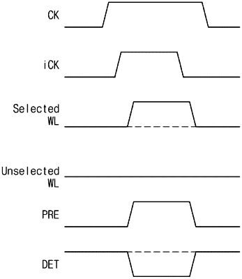
a word line driver connected with the selection lines, the word line driver connected with the rows of the memory cells through word lines, the word line driver configured to adjust voltages of the word lines in response to an internal clock signal and the voltages of the selection lines;
a detection circuit connected with the word lines, the detection circuit configured to activate a detection signal in response to the voltages of the word lines being identical at a specific timing; and
control circuitry that is configured to receive a command and an address from an external device and to notify the detection circuit of the specific timing based on activating a precharge signal.
|