| CPC G11C 11/4082 (2013.01) [G11C 7/106 (2013.01); G11C 7/1087 (2013.01); G11C 11/1673 (2013.01); G11C 11/1675 (2013.01); G11C 11/1697 (2013.01); G11C 11/4093 (2013.01)] | 13 Claims |
|
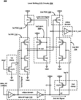
1. A level shifter comprising:
data control circuitry that provides activation signals in the first voltage domain;
logic circuitry that provides an output signal in a second voltage domain based on the activation signals in the first domain; and
latch circuitry that provides a latched control signal to a power-gate of the logic circuitry based on the activation signals so as to trigger activation of the logic circuitry to thereby provide the output signal in the second voltage domain,
wherein the logic circuitry includes a first power-gated switch as the power-gate and first inversion logic coupled in series between a source voltage supply in the second domain and ground, and wherein the logic circuitry includes a second power-gated switch and second inversion logic coupled in series between the source voltage supply in the second domain and ground, and
wherein the second inversion logic provides a buffered activation signal to the latch circuitry, and wherein the latch circuitry operates as a half-latch that receives the buffered activation signal and provides the latched control signal to the logic circuitry to activate the first power-gated switch.
|