| CPC G11C 11/4074 (2013.01) [G11C 7/109 (2013.01); G11C 7/12 (2013.01); G11C 8/12 (2013.01); G11C 11/4082 (2013.01); G11C 11/4085 (2013.01); G11C 11/4097 (2013.01); G11C 11/5628 (2013.01); G11C 16/0483 (2013.01); G11C 16/06 (2013.01); G11C 16/08 (2013.01); G11C 16/10 (2013.01); G11C 16/30 (2013.01); G11C 16/3436 (2013.01); G11C 2207/2209 (2013.01)] | 20 Claims |
|
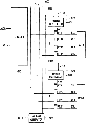
1. A nonvolatile memory device comprising:
a memory cell region including a first metal pad;
a peripheral circuit region including a second metal pad and vertically connected to the memory cell region by the first metal pad and the second metal pad;
a memory cell array in the memory cell region, the memory cell array including a plurality of mats corresponding to different word-lines, each of the plurality of mats including a plurality of cell strings connected to a plurality of word-lines, a plurality of bit-lines, a plurality of string selection lines and a ground selection line, wherein:
a first cell string of a first mat of the plurality of mats is connected to a plurality of first word-lines, a first bit-line, a first string selection line and a first ground selection line,
a second cell string of a second mat of the plurality of mats is connected to a plurality of second word-lines, a second bit-line, a second string selection line and a second ground selection line,
the first and second cell strings are perpendicular to a substrate respectively, and
each of the first and second cell strings includes at least one ground selection transistor, a plurality of memory cells, and a plurality of string selection transistors coupled in series; and
a row decoder in the peripheral circuit region, the row decoder connected to the plurality of first and second word-lines and configured to apply corresponding word-line voltages to the plurality of first and second word-lines through the first metal pad and the second metal pad,
wherein the row decoder is configured to:
apply a first voltage to a third word-line among the plurality of first and second word-lines when a read operation of the nonvolatile memory device is performed for only one of the first and second mats, and
apply a second voltage greater than the first voltage to the third word-line when the read operation is performed for both of the first and second mats simultaneously.
|