| CPC G11C 11/2275 (2013.01) [G11C 11/223 (2013.01); G11C 11/2273 (2013.01); H10B 51/30 (2023.02); H10B 51/40 (2023.02)] | 20 Claims |
|
1. A memory circuit comprising:
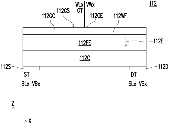
a memory array comprising a plurality of memory cells, each memory cell of the plurality of memory cells comprising:
an n-type channel layer comprising a metal oxide material; and
a gate structure overlying and adjacent to the n-type channel layer, the gate structure comprising a conductive layer overlying a ferroelectric layer,
wherein
the memory circuit is configured to apply a gate voltage to each memory cell of the plurality of memory cells in first and second write operations,
the gate voltage has a positive polarity and a first magnitude in the first write operation, and
the gate voltage has a negative polarity and a second magnitude greater than the first magnitude in the second write operation.
|