| CPC G11C 11/221 (2013.01) [H01L 21/76802 (2013.01); H01L 21/76805 (2013.01); H01L 21/76831 (2013.01); H01L 21/76895 (2013.01); H01L 23/5226 (2013.01); H01L 23/53209 (2013.01); H01L 23/53228 (2013.01); H01L 23/53242 (2013.01); H01L 23/53257 (2013.01); H01L 23/535 (2013.01); H01L 23/5381 (2013.01); H01L 23/5386 (2013.01); H01L 28/55 (2013.01); H01L 28/60 (2013.01); H01L 28/65 (2013.01); H03K 19/185 (2013.01); H10B 53/20 (2023.02); H10B 53/30 (2023.02)] | 20 Claims |
|
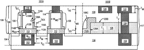
1. A device comprising:
a first region comprising:
a plurality of first conductive interconnects within a first level; and
a second level above the first level, the second level comprising:
a plurality of ferroelectric memory devices above a respective first conductive interconnect in the plurality of first conductive interconnects;
an electrode structure coupled between a respective ferroelectric memory device in the plurality of ferroelectric memory devices and the respective first conductive interconnect, the electrode structure comprising a first sidewall;
an encapsulation layer on a second sidewall of individual ones of the plurality of ferroelectric memory devices, wherein an outer third sidewall of the encapsulation layer is substantially aligned with the first sidewall; and
a via electrode on individual ones of the plurality of ferroelectric memory devices; and
a second region adjacent to the first region, the second region comprising an interconnect structure, the interconnect structure comprising:
one or more second conductive interconnects within the first level;
an etch stop layer comprising a dielectric material in the second level;
a plurality of metal lines above the etch stop layer, the plurality of metal lines in the second level; and
a via structure coupling a metal line in the plurality of metal lines with a second conductive interconnect in the one or more second conductive interconnects, wherein the via structure is in the second level and wherein an uppermost surface of the via electrode is co-planar with an uppermost surface of the plurality of metal lines.
|