| CPC G11C 11/161 (2013.01) [H10B 61/00 (2023.02); H10N 50/01 (2023.02); H10N 50/10 (2023.02); H10N 50/80 (2023.02); H10N 50/85 (2023.02)] | 18 Claims |
|
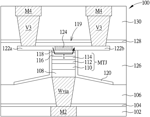
1. A bottom-pinned spin-orbit torque magnetic random access memory, comprising:
a substrate;
a bottom electrode layer on said substrate;
a magnetic tunnel junction on said bottom electrode layer;
a spin-orbit torque layer on said magnetic tunnel junction;
a capping layer on said spin-orbit torque layer, wherein said capping layer, said spin-orbit torque layer, said magnetic tunnel junction and said bottom electrode layer constitute a memory unit;
an injection layer on said capping layer, wherein said injection layer is divided into a first part and a second part, and said first part and said second part are connected respectively with two ends of said capping layer; and
an insulating layer between said first part and said second part of said injection layer, wherein a top surface of said insulating layer is flush with top surfaces of said first part and said second part of said injection layer.
|