| CPC G09G 5/10 (2013.01) [H04N 23/57 (2023.01); G09G 2300/0439 (2013.01); G09G 2310/0232 (2013.01); G09G 2320/0233 (2013.01)] | 20 Claims |
|
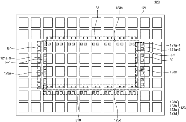
1. An electronic device, comprising:
a display panel including a plurality of pixel groups in a first region and a second region, the plurality of pixel groups including
first pixel groups in the first region, and
second pixel groups in the second region; and
a control circuit configured to
receive first image data,
generate second image data by adjusting gray values of the first image data corresponding to one or more pixel groups, wherein the one or more pixel groups are at least one of
one or more particular first pixel groups, which are a limited portion of the first pixel groups and that are adjacent to a boundary between the first region and the second region, or
one or more particular second pixel groups, which are limited portion of the second pixel groups and that are adjacent to the boundary, and
output the second image data to the display panel.
|