| CPC G09G 3/3677 (2013.01) [G06F 1/3265 (2013.01); G06F 3/038 (2013.01); G09G 3/3266 (2013.01); G11C 19/28 (2013.01); H01L 27/124 (2013.01); G09G 5/008 (2013.01); G09G 2300/0809 (2013.01); G09G 2300/0871 (2013.01); G09G 2310/0205 (2013.01); G09G 2310/0248 (2013.01); G09G 2310/0286 (2013.01); G09G 2310/08 (2013.01); G09G 2320/0247 (2013.01); G09G 2330/021 (2013.01)] | 7 Claims |
|
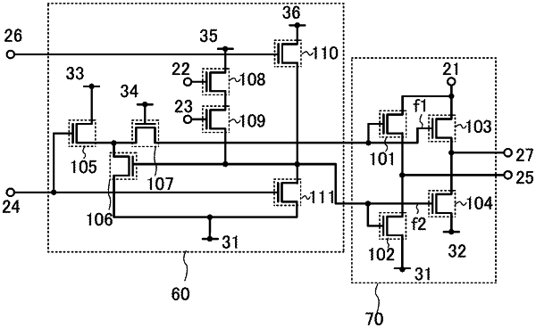
1. A semiconductor device comprising:
a first pulse output circuit comprising a first transistor, a second transistor, a third transistor, a fourth transistor, a fifth transistor, a sixth transistor, a seventh transistor, and an eighth transistor,
wherein one of a source and a drain of the first transistor is electrically connected to a first wiring,
wherein one of a source and a drain of the second transistor is electrically connected to the first wiring,
wherein one of a source and a drain of the third transistor is electrically connected to a second wiring,
wherein one of a source and a drain of the fourth transistor is electrically connected to the second wiring,
wherein one of a source and a drain of the fifth transistor is electrically connected to one of a source and a drain of the sixth transistor,
wherein one of a source and a drain of the seventh transistor is electrically connected to one of a source and a drain of the eighth transistor,
wherein the other of the source and the drain of the first transistor is electrically connected to a third wiring,
wherein the other of the source and the drain of the third transistor is electrically connected to the third wiring,
wherein the other of the source and the drain of the second transistor is electrically connected to a fourth wiring,
wherein the other of the source and the drain of the sixth transistor is electrically connected to the fourth wiring,
wherein the other of the source and the drain of the eighth transistor is electrically connected to the fourth wiring,
wherein the other of the source and the drain of the fourth transistor is electrically connected to a fifth wiring,
wherein the other of the source and the drain of the fifth transistor is electrically connected to a sixth wiring,
wherein the other of the source and the drain of the seventh transistor is electrically connected to a seventh wiring,
wherein a gate of the first transistor is electrically connected to a gate of the third transistor,
wherein the gate of the first transistor is electrically connected to the one of the source and the drain of the fifth transistor,
wherein the gate of the first transistor is electrically connected to the one of the source and the drain of the sixth transistor,
wherein a gate of the second transistor is electrically connected to a gate of the fourth transistor,
wherein the gate of the second transistor is electrically connected to the one of the source and the drain of the seventh transistor,
wherein the gate of the second transistor is electrically connected to the one of the source and the drain of the eighth transistor,
wherein a gate of the fifth transistor is electrically connected to an eighth wiring which is configured to supply a start pulse, and
wherein a gate of the eighth transistor is directly connected to the eighth wiring.
|