| CPC G09G 3/3607 (2013.01) [G02F 1/136286 (2013.01); G02F 1/1368 (2013.01); G09G 3/3688 (2013.01); H01L 27/124 (2013.01); G09G 2330/021 (2013.01)] | 18 Claims |
|
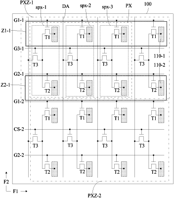
1. A display panel, comprising:
a base substrate;
a plurality of sub-pixels on the base substrate, wherein at least one of the plurality of sub-pixels comprises a pixel electrode;
a plurality of transistors, comprising a plurality of first transistors, a plurality of second transistors and a plurality of third transistors;
a plurality of data lines, disposed on the base substrate at intervals; and
a plurality of gate lines, disposed on the base substrate at intervals, and comprising a plurality of first gate lines, a plurality of second gate lines and a plurality of third gate lines; wherein:
two adjacent rows of sub-pixels are taken as a row group, and the row group has a first sub row group and a second sub row group arranged in a column direction; the pixel electrode comprises a first pixel electrode and a second pixel electrode;
one sub-pixel in the first sub row group comprises one first transistor of the plurality of first transistors and one first pixel electrode; wherein a gate electrode of the first transistor in the first sub row group is electrically connected with one first gate line of the plurality of first gate lines; in the same sub-pixel, a second electrode of the first transistor is electrically connected with the first pixel electrode;
one sub-pixel in the second sub row group comprises one second transistor of the plurality of second transistors and one second pixel electrode; wherein a gate electrode of the second transistor in the second sub row group is electrically connected with one second gate line of the plurality of second gate lines; in the same sub-pixel, a second electrode of the second transistor is electrically connected with the second pixel electrode;
in the same row group, two adjacent sub-pixels in the column direction share one third transistor of the plurality of third transistors; wherein a gate electrode of the third transistor in the row group is electrically connected to one third gate line of the plurality of third gate lines; and
the first transistor and the second transistor in one column of sub-pixels are electrically connected with one data line of the plurality of data lines through the shared third transistor;
wherein an active layer of the third transistor comprises a first source electrode region, a first drain electrode region, a second drain electrode region, a first channel region and a second channel region;
wherein the first channel region is between the first source electrode region and the first drain electrode region, and the second channel region is between the first source electrode region and the second drain electrode region; and
the first source electrode region is electrically connected with the data line, the first drain electrode region is electrically connected with a first electrode of the first transistor, and the second drain electrode region is electrically connected with a first electrode of the second transistor.
|