| CPC G09G 3/36 (2013.01) [G09G 2300/0842 (2013.01); G09G 2310/0289 (2013.01); G09G 2310/08 (2013.01); G09G 2330/028 (2013.01)] | 20 Claims |
|
1. A system for generating and supplying a voltage to a pixel array, said system comprising:
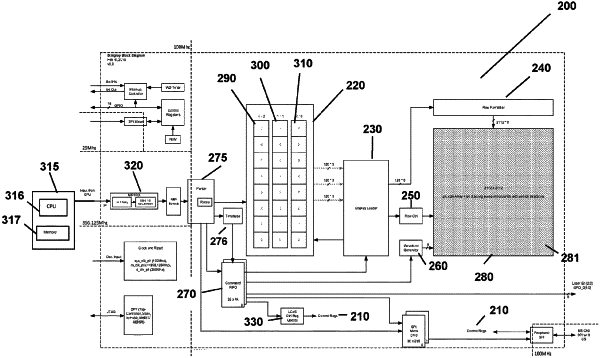
a plurality of display pixels forming the pixel array, each display pixel comprising a pixel circuit for driving the pixel and the pixel circuit including a plurality of data latches and an output latch, the pixel array being a liquid crystal on silicon array, said liquid crystal on silicon array comprising a liquid crystal layered between two substrates;
a row formatter configured to store a plurality of bits representing image data for a row of display pixels of the pixel array;
a row controller configured to write a subset of the plurality of bits representing image data for a display pixel of the row into the plurality of data latches of said pixel circuit; and
a waveform generator for generating reference pulses represented by a set of reference bits and wherein a number of the set of reference bits is equal to or corresponds to a number of bits stored in the data latches of each pixel circuit, the waveform generator being connected to each pixel via a Global Modulation Bus (G-bus) having a width equal to the number of bits stored in the latches of each pixel circuit, the waveform generator being configured to send out a word of memory contents on the G-bus periodically in sequence to generate a plurality of voltage pulses equal to the width of the G-bus on different G-bus lines of the G-bus, and wherein:
a voltage pulse on a G-bus line of the G-bus may be divided across several G-bus lines:
a duration of each voltage pulse on each line of the G-bus is programmable; and
the duration of the voltage pulses is substantially shorter than a Liquid Crystal response time;
wherein the pixel circuit is configured to:
compare each reference bit to corresponding bits stored in the data latches of each pixel circuit, and generate a voltage at an electrode of each pixel based on this comparison, all the bits stored in the data latches of the pixel circuit being compared to their corresponding bits stored in the waveform generator within a time period shorter than the Liquid Crystal response time;
input a bit “1” to the output latch if the corresponding bit stored in the data latch is equal to “1”; and
input a bit “0” to the output latch when a Gset signal output from the waveform generator is applied to the output latch.
|