| CPC G09G 3/3266 (2013.01) [G11C 19/28 (2013.01); G09G 2300/0426 (2013.01); G09G 2310/0286 (2013.01); G09G 2310/061 (2013.01); G09G 2310/08 (2013.01)] | 19 Claims |
|
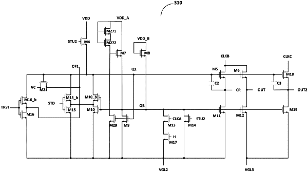
1. A shift register unit, comprising a blanking unit, a first transmission circuit, and a first input-output unit,
wherein the blanking unit is configured to charge a pull-up control node in response to a compensation selection control signal and input a blanking pull-up signal to a blanking pull-up node;
the first input-output unit comprises a first pull-up node and a first output terminal;
the first transmission circuit is electrically connected to the blanking pull-up node and the first pull-up node, and is configured to charge the first pull-up node, by using the blanking pull-up signal, in response to a first transmission signal;
the first input-output unit comprises an output circuit, a first pull-down control circuit, and a first pull-down auxiliary control circuit,
wherein the output circuit is configured to output a composite output signal to the first output terminal under control of a level of the first pull-up node;
the first pull-down control circuit is configured to control a level of a pull-down node under the control of the level of the first pull-up node;
the first pull-down auxiliary control circuit is configured to control the first pull-down control circuit so as to further control a level of the pull-down node under the control of the level of the first pull-up node;
the first pull-down control circuit comprises a seventh transistor and a ninth transistor, a gate electrode of the seventh transistor is connected to a first electrode of the seventh transistor and is further configured to be connected to a third voltage terminal to receive a third voltage, and a second electrode of the seventh transistor is connected to the pull-down node;
a gate electrode of the ninth transistor is connected to the first pull-up node, a first electrode of the ninth transistor is connected to the pull-down node, and a second electrode of the ninth transistor is connected to a fifth voltage terminal to receive a fifth voltage;
the first pull-down auxiliary control circuit comprises an auxiliary control switching circuit and an auxiliary control transistor;
a gate electrode of the auxiliary control switching circuit is configured to be connected with the third voltage terminal to receive the third voltage, and the auxiliary control switching circuit is connected between the third voltage terminal and the gate electrode of the seventh transistor; and
a gate electrode of the auxiliary control transistor is connected to the first pull-up node, a first electrode of the auxiliary control transistor is connected to the gate electrode of the seventh transistor and is connected with the auxiliary control switching circuit, and a second electrode of the auxiliary control transistor is connected to the fifth voltage terminal to receive the fifth voltage.
|