| CPC G09G 3/3233 (2013.01) [G09G 2300/0804 (2013.01); G09G 2300/0842 (2013.01); G09G 2300/0861 (2013.01); G09G 2310/08 (2013.01)] | 10 Claims |
|
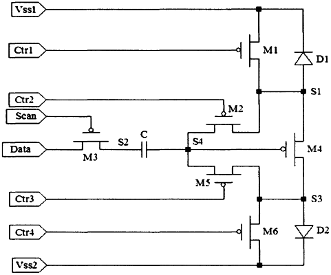
1. A pixel driving circuit, applied to a display panel provided with a pixel array, the pixel array comprising a first light-emitting device and a second light-emitting device adjacent to each other and located on a same column, wherein:
an anode of the first light-emitting device is connected to a first node and a cathode of the first light-emitting device is connected to a first supply voltage;
an anode of the second light-emitting device is connected to a third node and a cathode of the second light-emitting device is connected to a second supply voltage;
the pixel driving circuit comprises a first thin film transistor, a second thin film transistor, a third thin film transistor, a fourth thin film transistor, a fifth thin film transistor, a sixth thin film transistor and a capacitor;
a controlled end of the first thin film transistor is connected to a first control signal, a first end of the first thin film transistor is connected to the first supply voltage and a second end of the first thin film transistor is connected to the first node;
a controlled end of the second thin film transistor is connected to a second control signal, a first end of the second thin film transistor is connected to a fourth node and a second end of the second thin film transistor is connected to the second end of the first thin film transistor;
a controlled end of the third thin film transistor is connected to a scanning signal, a first end of the third thin film transistor is connected to a data signal and a second end of the third thin film transistor is connected to a second node;
a controlled end of the fourth thin film transistor is connected to the fourth node, a first end of the fourth thin film transistor is connected to the first node and a second end of the fourth thin film transistor is connected to a third node;
a controlled end of the fifth thin film transistor is connected to a third control signal, a first end of the fifth thin film transistor is connected to the fourth node and a second end of the fifth thin film transistor is connected to the third node;
a controlled end of the sixth thin film transistor is connected to a fourth control signal, a first end of the sixth thin film transistor is connected to the second end of the fifth thin film transistor, a second end of the sixth thin film transistor is connected to the second supply voltage; and
an end of the capacitor is connected to the second node and another end of the capacitor is connected to the fourth node.
|