| CPC G09G 3/3233 (2013.01) [G09G 3/3266 (2013.01); G09G 2300/0842 (2013.01); G09G 2310/08 (2013.01); G09G 2320/0233 (2013.01); G09G 2330/021 (2013.01)] | 15 Claims |
|
1. A display panel, comprising:
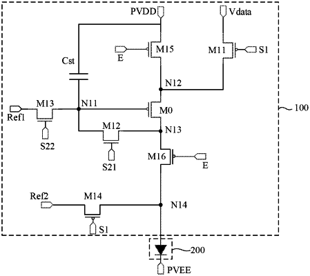
pixel groups, wherein each pixel group of the pixel groups comprises B pixel rows, where B≥2, and B is an integer; and each pixel row of the B pixel rows comprises pixel driving circuits, wherein each of the pixel driving circuits comprises a driving transistor, a data writing control terminal, and a first scanning control terminal, wherein the driving transistor comprises a control electrode electrically connected to a first node, and a first electrode electrically connected to a second node; and
first scanning driving units, one of the first scanning driving units being electrically connected to the first scanning control terminals of the pixel driving circuits in one pixel group of the pixel groups,
wherein a working cycle of each of the pixel driving circuits comprises a data writing phase, wherein, during the data writing phase, the data writing control terminal is configured to receive an effective level, and the one of first scanning driving units is configured to provide an effective level to the first scanning control terminals; and
wherein the pixel driving circuits in one pixel group of the pixel groups comprise a first pixel driving circuit and a second pixel driving circuit, wherein in a display duration of a frame of an image, the data writing phase of the first pixel driving circuit is prior to the data writing phase of the second pixel driving circuit; and in a case where the first pixel driving circuit and the second pixel driving circuit receive a same data voltage, a potential VN11 of the first node in the first pixel driving circuit after the data writing phase of the first pixel driving circuit is greater than a potential VN12 of the first node in the second pixel driving circuit after the data writing phase of the second pixel driving circuit.
|