| CPC G09G 3/32 (2013.01) [G09G 2310/0267 (2013.01); G09G 2310/0275 (2013.01); G09G 2320/0247 (2013.01)] | 20 Claims |
|
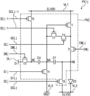
1. A display device comprising:
a display panel including a pixel, the pixel including:
a light-emitting element;
a first transistor which is connected between a first voltage line which receives a first driving voltage and the light-emitting element, and operates in response to a potential of a first node;
a second transistor which is connected between a data line and the first node and receives a first scan signal;
a first capacitor connected between the first node and a second node;
a third transistor which is connected between the first transistor and the first node and receives a second scan signal;
a fourth transistor which is connected between a reference voltage line which receives a reference voltage and the first node and receives a third scan signal;
a fifth transistor which is connected between the first transistor and the second node and receives an emission control signal;
a sixth transistor which is connected between the first voltage line and a third node and receives a fourth scan signal; and
a seventh transistor which is connected between the first node and the third transistor and receives a fifth scan signal; and
a panel driver which drives the display panel.
|