| CPC G09G 3/32 (2013.01) [G09G 2300/043 (2013.01); G09G 2300/0819 (2013.01); G09G 2320/0233 (2013.01); G09G 2320/045 (2013.01)] | 20 Claims |
|
1. A display panel, comprising:
a pixel circuit and a light-emitting element,
wherein the pixel circuit comprises a drive module, a data write transistor, a bias transistor and a reset module;
wherein the drive module comprises a drive transistor;
wherein the reset module is connected to an gate of the drive transistor;
wherein the data write transistor is configured to transmit a data signal, and the bias transistor is configured to transmit a bias signal;
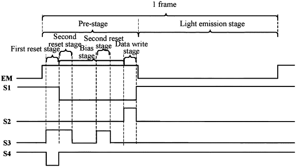
wherein an operation of the pixel circuit comprises at least one bias stage and at least one reset stage, during the bias stage, the bias transistor is on and provides the bias signal, during the reset stage, the reset module provides a reset signal for a gate of the drive transistor; and
wherein a time period of the reset stage at least partially overlaps a time period of the bias stage;
the reset stage comprises a first reset stage and a second reset stage; and
a time period of the first reset stage does not overlap a time period of the bias stage, and a time period of the second reset stage at least partially overlaps the time period of the bias stage; or
before the bias stage ends, the gate of the drive transistor is disconnected from the reset signal, and then the bias stage ends.
|