| CPC G09G 3/32 (2013.01) [G09G 3/2007 (2013.01); H01L 25/18 (2013.01); H01L 27/156 (2013.01); G09G 2300/0452 (2013.01); H01L 24/05 (2013.01); H01L 24/08 (2013.01); H01L 24/13 (2013.01); H01L 24/16 (2013.01); H01L 24/48 (2013.01); H01L 24/73 (2013.01); H01L 24/81 (2013.01); H01L 2224/05573 (2013.01); H01L 2224/05582 (2013.01); H01L 2224/05611 (2013.01); H01L 2224/05624 (2013.01); H01L 2224/05644 (2013.01); H01L 2224/05647 (2013.01); H01L 2224/05687 (2013.01); H01L 2224/08148 (2013.01); H01L 2224/13082 (2013.01); H01L 2224/13111 (2013.01); H01L 2224/13124 (2013.01); H01L 2224/13144 (2013.01); H01L 2224/13147 (2013.01); H01L 2224/16145 (2013.01); H01L 2224/48157 (2013.01); H01L 2224/73207 (2013.01); H01L 2224/80801 (2013.01); H01L 2224/81801 (2013.01)] | 18 Claims |
|
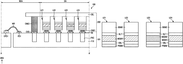
1. A display device comprising:
a substrate;
a plurality of pixel electrodes on the substrate and spaced apart from each other;
a plurality of light-emitting elements on the plurality of pixel electrodes, respectively; and
a common electrode layer on the plurality of light-emitting elements and to which a common voltage is applied,
wherein the plurality of light-emitting elements comprise a first light-emitting element configured to emit first light according to a first driving current and a second light-emitting element configured to emit second light according to a second driving current, the first light having a different wavelength than the second light, and
wherein an active layer of the first light-emitting element has a same material as an active layer of the second light-emitting element,
wherein a current density of the first driving current is lower than a current density of the second driving current, and
wherein an application period of the first driving current is configured to be adjusted according to the gray level of the first light-emitting element, and an application period of the second driving current is configured to be adjusted according to the gray level of the second light-emitting element.
|