| CPC G09G 3/2074 (2013.01) [G09G 2310/0297 (2013.01); G09G 2320/0276 (2013.01); G09G 2320/0673 (2013.01)] | 24 Claims |
|
1. A source driver, comprising:
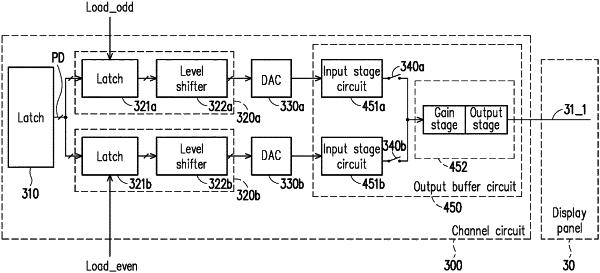
a plurality of channel circuits, each of the channel circuits comprising:
an output buffer circuit, having a first input terminal, a second input terminal and an output terminal, wherein the output terminal of the output buffer circuit is configured to output a driving voltage according to a gamma voltage to a data line of a display panel in a scan line period;
a first digital-to-analog converter and a second digital-to-analog converter, wherein an output terminal of the first digital-to-analog converter is coupled to the first input terminal of the output buffer circuit, and an output terminal of the second digital-to-analog converter is coupled to the second input terminal of the output buffer circuit;
a first switch, disposed along a first signal path between the output terminal of the first digital-to-analog converter and the output terminal of the output buffer circuit; and
a second switch, disposed along a second signal path between the output terminal of the second digital-to-analog converter and the output terminal of the output buffer circuit,
wherein when a value of pixel data falls within a first sub-range, the first digital-to-analog converter is configured to convert the pixel data to output a first gamma voltage which falls in a first output voltage range, and
when the value of the pixel data falls within second sub-range, the second digital-to-analog converter is configured to convert the pixel data to output a second gamma voltage which falls in a second output voltage range,
wherein the first output voltage range of the first digital-to-analog converter is different from the second output voltage range of the second digital-to-analog converter.
|