| CPC G09G 3/20 (2013.01) [G09G 2310/0286 (2013.01); G09G 2310/0297 (2013.01); G09G 2330/021 (2013.01)] | 20 Claims |
|
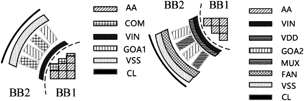
1. A display panel comprising a display area and a non-display area surrounding the display area, the display panel comprising:
a pixel array, an edge of which defines a boundary between the display area and the non-display area, wherein the non-display area comprises a first area and a second area arranged in sequence in a direction away from the pixel array, such that the second area is farther from the pixel array than the first area;
a compensation circuit configured to compensate for a parasitic capacitance of pixel in the pixel array, and the compensation circuit comprising a first portion located in the first area and a second portion located in the second area; and
a first shift register located in the second area;
wherein the second portion of the compensation circuit is aligned with the first shift register circuit in a circumferential direction of the pixel array.
|