| CPC G09G 3/20 (2013.01) [G09G 2300/0852 (2013.01); G09G 2310/0202 (2013.01); G09G 2320/0247 (2013.01); G09G 2320/08 (2013.01)] | 17 Claims |
|
1. A driving method of a display panel, wherein the display panel comprises:
a plurality of scan lines;
a plurality of data lines, wherein the data lines and the scan lines are disposed in an array in a display region of the display panel;
a gate driving circuit electrically connected to the scan lines correspondingly, and disposed in a non-display region of the display panel; and
a plurality of pixels disposed at intersections of each of the scan lines and each of the data lines, respectively;
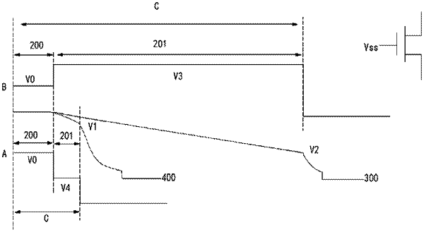
wherein when the display panel displays images, during a display period of a frame of image, when a displayed image of the display panel is subjected to frequency switching, a data voltage of the data lines or a switching voltage of the pixels is changed synchronously with the frequency switching of the displayed image;
wherein during the display period of the frame of image, the display period of the frame of image comprises a first stage and a second stage, the first stage and the second stage are alternated in sequence, and a duration of the first stage is different from a duration of the second stage;
wherein when the display panel is switched from a low frequency signal to a high frequency signal, a value of the data voltage is increased in the second stage, and the value of the data voltage in the second stage is greater than a corresponding value of the data voltage in the first stage, and wherein when the display panel is switched from the high frequency signal to the low frequency signal, the value of the data voltage is reduced in the second stage, and the value of the data voltage in the second stage is less than the corresponding value of the data voltage in the first stage.
|