| CPC G06N 10/00 (2019.01) [H01L 29/66977 (2013.01); H10N 60/01 (2023.02); H10N 60/128 (2023.02)] | 15 Claims |

|
1. A method for producing a quantum device, comprising:
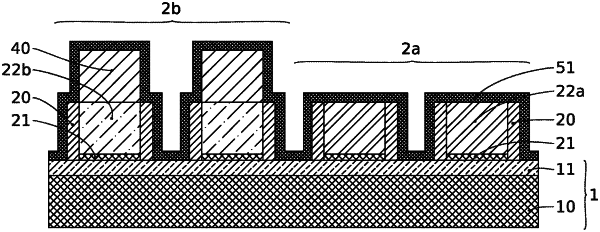
providing a substrate having a front face and carrying a transistor pattern on the front face thereof, said transistor pattern comprising, in a stack:
a gate dielectric on the front face of the substrate, and
a gate on the gate dielectric, said gate having a top and sidewalls,
forming a protective layer at the front face of the substrate, said protective layer being configured to prevent diffusion of at least one metal species in the substrate,
forming a metal layer based on at least one metal species at least on the sidewalls of the gate, and
forming a superconducting region in the gate by lateral diffusion of the at least one metal species from the sidewalls of said gate.
|