| CPC G06K 19/07775 (2013.01) [G06K 19/025 (2013.01); G06K 19/072 (2013.01); G06K 19/07722 (2013.01); G06K 19/07779 (2013.01); H01Q 1/2208 (2013.01); H01Q 1/38 (2013.01)] | 13 Claims |
|
1. A device, comprising:
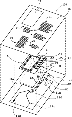
a substrate;
a plurality of switches disposed on said substrate and interrupted in an initial state;
a plurality of near-field communication (NFC) chips each respectively assigned to at least one of said switches;
a NFC antenna;
said switches and said NFC chips assigned to said switches being connected to one another in series resulting in individual series circuits being created, respectively each containing one of said switches and an NFC chip of said NFC chips assigned to said one switch, and being connected in each case to said NFC antenna;
a label having a film-shaped main body, said label joined face to face with said substrate;
said NFC chips are disposed on said label;
said switches are disposed on said substrate in a region different from a region joined by said label;
conductor tracks electrically connecting said switches, said NFC chips and said NFC antenna disposed on said substrate and said label; and
mutually facing contact points, which establish an electrically conducting contact between said conductor tracks on said label and on said substrate, are disposed on said label and on said substrate.
|