| CPC G06F 9/3887 (2013.01) [G06F 9/3001 (2013.01); G06F 9/30101 (2013.01); G06F 12/0284 (2013.01); G06F 13/1668 (2013.01); G06F 13/287 (2013.01); G06F 13/4068 (2013.01); G06F 15/7821 (2013.01); G06N 3/045 (2023.01); G06N 3/063 (2013.01); G06F 2212/1028 (2013.01)] | 20 Claims |
|
1. A device comprising:
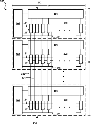
a plurality of computational memory banks, each computational memory bank of the plurality of computational memory banks including an array of memory units and a plurality of processing elements connected to the array of memory units; and
a plurality of single instruction, multiple data (SIMD) controllers, each SIMD controller of the plurality of SIMD controllers being contained within at least one computational memory bank of the plurality of computational memory banks;
wherein each SIMD controller is to provide instructions to the at least one computational memory bank and control execution of the instructions by the at least one computational memory bank;
wherein each processing element of the plurality of processing elements includes registers and an arithmetic logic unit (ALU) to perform operations with the registers; and
wherein each processing element of the plurality of processing elements is to receive communicated state from registers of another processing element, the ALU to perform operations with the registers and the communicated state.
|