| CPC G06F 7/503 (2013.01) [G06F 7/502 (2013.01); G06F 9/3001 (2013.01); G06F 9/30029 (2013.01); H03K 19/0021 (2013.01); H03K 19/018521 (2013.01)] | 20 Claims |
|
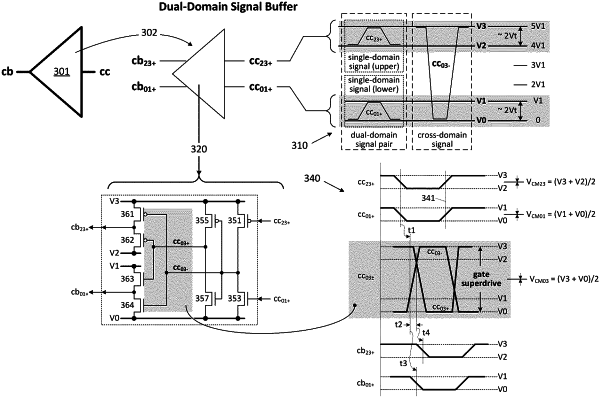
1. Signal driver circuitry within an integrated circuit device, the signal driver comprising:
first and second transistors having drain terminals coupled to one another, source terminals coupled respectively to upper and lower supply voltage nodes of a first voltage domain, and gate terminals coupled respectively to first and second control signal lines; and
third and fourth transistors having drain terminals coupled to one another and source terminals coupled respectively to upper and lower supply voltage nodes of a second voltage domain, the third transistor having a gate terminal coupled to one of the first and second control signal lines and the fourth transistor having a gate terminal coupled to the other of the first and second control signal lines.
|