| CPC G06F 3/0608 (2013.01) [G06F 3/064 (2013.01); G06F 3/0673 (2013.01)] | 20 Claims |

|
11. A circuit arrangement comprising:
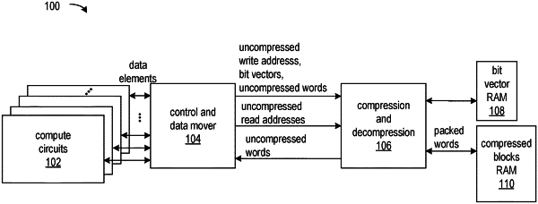
a first random access memory (RAM)
a write compression circuit configured to:
pack non-zero data elements of a succession of words of a plurality of uncompressed blocks into packed words, by performing operations of:
packing non-zero data elements of one or more words of the succession in each packed word,
restricting each packed word to data elements of one uncompressed block of the plurality of uncompressed blocks, and
writing each packed word in the RAM and within a compressed address range associated with the one uncompressed block, wherein the writing includes initiating the writing in response to the packed word being full of non-zero data elements, or initiating the writing before the packed word is full of non-zero data elements of the one uncompressed block of the plurality of uncompressed blocks, in response to a next input word of the succession being of another uncompressed block of the plurality of uncompressed blocks.
|