| CPC G06F 3/0446 (2019.05) [G06F 3/0412 (2013.01); G06F 3/04164 (2019.05); G06F 2203/04112 (2013.01)] | 25 Claims |
|
1. A touch display device, comprising:
a display panel having thereon an active area;
an encapsulation layer on the active area;
a transistor under the encapsulation layer, the transistor including a gate electrode, and a source or drain electrode;
a plurality of touch electrodes on an active area of the display panel, and disposed on the encapsulation layer;
a plurality of touch link lines located outside of the active area, and electrically coupled to at least one of the plurality of touch electrodes;
a plurality of pad lines electrically coupled to each of the plurality of touch link lines; and
a plurality of touch pads electrically coupled to each of the plurality of pad lines,
wherein the plurality of touch pads include:
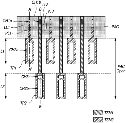
a plurality of first touch pads located on a first region, and electrically coupled to each of a plurality of first pad lines among the plurality of pad lines, the plurality of first pad lines and the plurality of first touch pads disposed on a same layer; and
a plurality of second touch pads located on a second region located farther from the plurality of touch link lines than the first region, and electrically coupled to each of a plurality of second pad lines among the plurality of pad lines, the plurality of second pad lines each at least partially disposed on a layer different from a layer where the plurality of second touch pads are disposed and different from the layer where the plurality of first pad lines are disposed, and the plurality of second touch pads disposed on the same layer as the plurality of first touch pads,
wherein the plurality of first touch pads are in a same layer as the source or drain electrode of the transistor, and
wherein the touch display device further comprises a first insulation layer between the layer of the plurality of first pad lines and the layer of the plurality of second pad lines.
|