| CPC G06F 3/04166 (2019.05) [G06F 1/1643 (2013.01); G06F 3/044 (2013.01); G06F 3/0443 (2019.05); G09G 3/3233 (2013.01); G09G 2354/00 (2013.01)] | 20 Claims |
|
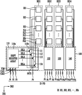
16. A display device comprising:
a display panel in which a base layer, a circuit element layer, a display element layer, and a thin film encapsulation layer (TFE) are sequentially stacked; and
an input sensor disposed on the thin film encapsulation layer, wherein the input sensor comprises:
a plurality of sensing electrodes; and
a plurality of multiplexers, where each multiplexer connects one group of the sensing electrodes to one output terminal,
wherein each of the multiplexers comprises:
a multiplexer circuit including a plurality of switching transistors; and
a shift register array for outputting selection signals for controlling the plurality of switching transistors,
wherein each of the switching transistors includes sub-switching transistors connected in parallel between one of the sensing electrodes corresponding to the one group and the output terminal,
wherein for each multiplexer circuit, sub-switching transistors are sequentially turned on in response to sequential selection signals from a corresponding shift register array.
|