| CPC G06F 21/62 (2013.01) [G01R 31/31719 (2013.01); G01R 31/31855 (2013.01); G01R 31/318572 (2013.01); G06F 21/50 (2013.01); G06F 21/70 (2013.01)] | 18 Claims |
|
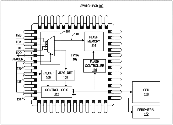
1. A field-programmable gate array (FPGA) chip mounted on a printed circuit board (PCB), comprising:
a joint test action group (JTAG) interface comprising a number of input/output (I/O) pins and an enablement pin;
a control logic block coupled to the enablement pin of the JTAG interface, wherein the control logic block is to receive a control signal from an off-chip control unit and control a logical value of the enablement pin based on the received control signal, thereby facilitating the off-chip control unit to lock or unlock the JTAG interface; and
a detection logic block to detect an unauthorized access to the FPGA chip, wherein an input to the detection logic is coupled to the enablement pin, and wherein a conductive trace coupling the input of the detection logic block and the enablement pin is situated on an inner layer of the PCB;
wherein an output of the control logic block and the enablement pin is coupled via a conductive trace situated on a top layer of the PCB, and wherein the conductive trace comprises a detachable resistor to allow the control logic block to decouple from the FPGA chip during development of the FPGA chip.
|