| CPC G06F 12/128 (2013.01) [G06F 9/3001 (2013.01); G06F 9/30043 (2013.01); G06F 9/30047 (2013.01); G06F 9/546 (2013.01); G06F 11/1064 (2013.01); G06F 12/0215 (2013.01); G06F 12/0238 (2013.01); G06F 12/0292 (2013.01); G06F 12/0802 (2013.01); G06F 12/0804 (2013.01); G06F 12/0806 (2013.01); G06F 12/0811 (2013.01); G06F 12/0815 (2013.01); G06F 12/082 (2013.01); G06F 12/0853 (2013.01); G06F 12/0855 (2013.01); G06F 12/0864 (2013.01); G06F 12/0884 (2013.01); G06F 12/0888 (2013.01); G06F 12/0891 (2013.01); G06F 12/0895 (2013.01); G06F 12/0897 (2013.01); G06F 12/12 (2013.01); G06F 12/121 (2013.01); G06F 12/126 (2013.01); G06F 12/127 (2013.01); G06F 13/1605 (2013.01); G06F 13/1642 (2013.01); G06F 13/1673 (2013.01); G06F 13/1689 (2013.01); G06F 15/8069 (2013.01); G11C 5/066 (2013.01); G11C 7/10 (2013.01); G11C 7/1015 (2013.01); G11C 7/106 (2013.01); G11C 7/1075 (2013.01); G11C 7/1078 (2013.01); G11C 7/1087 (2013.01); G11C 7/222 (2013.01); G11C 29/42 (2013.01); G11C 29/44 (2013.01); G06F 2212/1016 (2013.01); G06F 2212/1021 (2013.01); G06F 2212/1024 (2013.01); G06F 2212/1041 (2013.01); G06F 2212/1044 (2013.01); G06F 2212/301 (2013.01); G06F 2212/454 (2013.01); G06F 2212/6032 (2013.04); G06F 2212/6042 (2013.01); G06F 2212/608 (2013.01); G06F 2212/62 (2013.01)] | 20 Claims |
|
1. An apparatus comprising:
a cache memory that includes a first memory bank and a second memory bank;
an interface configured to be coupled to a central processing unit, the interface to obtain a write operation from the central processing unit that specifies to write a first set of data to the first memory bank and a second set of data to the second memory bank;
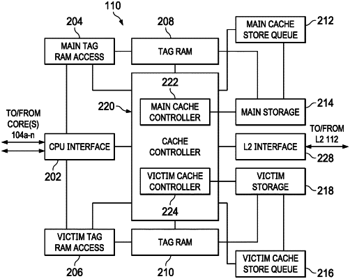
a cache controller coupled between the interface and the cache memory; and
bank processing logic coupled to the cache controller, the bank processing logic to:
determine that the first set of data corresponds to a data width of the first memory bank and that the second set of data is less than a data width of the second memory bank;
provide a first instruction to the cache controller to perform a partial read-modify-write operation to write the first set of data to the first memory bank; and
provide a second instruction to the cache controller to perform a full read-modify-write operation to write the second set of data to the second memory bank.
|