| CPC G06F 12/1009 (2013.01) [G06F 12/0238 (2013.01); G06F 12/1063 (2013.01); G06F 12/1408 (2013.01)] | 16 Claims |
|
1. A processor comprising:
a processor core to receive a read or write memory operation comprising a virtual memory address, wherein the virtual memory address comprises a plurality of memory tag bits; and
a memory management unit (MMU), the MMU to:
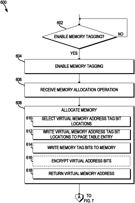
access a page table entry based on the virtual memory address, wherein the page table entry comprises a plurality of page tag bits;
determine whether to abort the read or write memory operation based on a comparison between the plurality of page tag bits to the plurality of memory tag bits;
select one or more of the plurality of memory tag bits based on the plurality of page tag bits using a mapping, wherein the mapping maps one or more inputs to the one or more of the plurality of memory tag bits, wherein the one or more inputs comprises the plurality of page tag bits, wherein, for each of the plurality of memory tag bits, the mapping maps at least one possible combination of the one or more inputs to a selection that includes the corresponding memory tag bit, wherein the one or more selected bits of the plurality of memory tag bits is fewer bits than the plurality of memory tag bits; and
send the read or write memory operation to a memory connected to the processor with the one or more selected bits of the plurality of memory tag bits.
|