| CPC G06F 12/0875 (2013.01) [G06F 13/124 (2013.01); G06F 13/1636 (2013.01); G06F 13/1689 (2013.01); G06F 9/3001 (2013.01); G06F 9/30098 (2013.01); G06F 2212/452 (2013.01)] | 26 Claims |
|
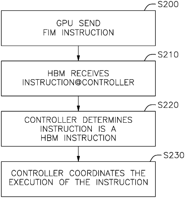
1. A method of processing in-memory commands in a high-bandwidth memory (HBM) system, the method comprising:
sending, by an HBM memory controller of a processor, a function-in-HBM (FIM) instruction to an HBM, wherein the FIM instruction comprises an atomic operation generated by the processor by merging a first instruction of a first type and a second instruction of a second type into an atomic instruction;
receiving the FIM instruction at a logic component of the HBM, wherein the logic component comprises: a controller, an Arithmetic Logic Unit (ALU), and a SRAM configured as a scratchpad; and
coordinating execution of the atomic operation of the FIM instruction, by the logic component using the controller and at least one of a DRAM, the ALU, or the SRAM.
|