| CPC G06F 11/1068 (2013.01) [G06F 3/0619 (2013.01); G06F 3/064 (2013.01); G06F 3/0656 (2013.01); G06F 3/0679 (2013.01); G06F 11/0757 (2013.01); G06F 11/1489 (2013.01)] | 17 Claims |
|
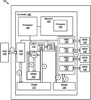
1. An apparatus comprising:
a controller for a memory device, the controller configured to:
accumulate, in a memory buffer, combined parity data for a plurality of regions of memory of the memory device in response to write operations for the plurality of regions of memory;
perform a recovery operation for a region of the plurality of regions in response to determining that a latency setting for the region satisfies a latency threshold, the recovery operation performed proactively, prior to receiving a read request, wherein the latency setting comprises a disabled extended error recovery setting; and
service the read request for data from the region based on the recovery operation to satisfy the latency setting.
|