| CPC G06F 1/3296 (2013.01) [G06F 1/28 (2013.01); H02M 1/0058 (2021.05); H02M 1/083 (2013.01); H02M 3/158 (2013.01)] | 20 Claims |
|
13. A method comprising:
reducing a quiescent power consumed by a phase of a core supply by configuring the phase to:
receive a pulse width modulated (PWM) signal;
generate an output current according to the PWM signal;
sense the output current;
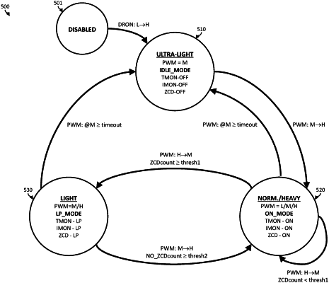
detect a presence or absence of a ZCD point in the output current during each PWM cycle of the PWM signal;
compute a ZCD count as a running total of consecutive PWM cycles having detected ZCD points;
compute a NO_ZCD count as a running total of consecutive PWM cycles having no ZCD point;
time a timeout period after a ZCD point when the ZCD point is detected in a PWM cycle;
determine a load condition based on the ZCD count, the NO_ZCD count, and the timeout period; and
selected an operating mode from a plurality of possible operating modes based on the load condition.
|