| CPC G06F 1/28 (2013.01) [G06F 1/3275 (2013.01); G06F 1/3287 (2013.01); G06F 13/4273 (2013.01); G11C 5/063 (2013.01)] | 20 Claims |
|
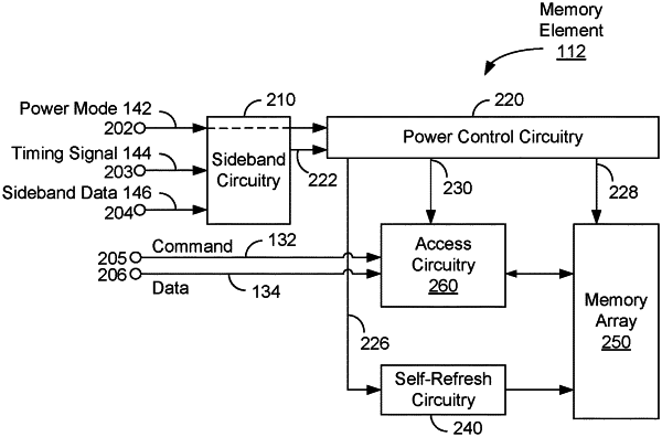
1. A host device for controlling operation of a multi-element device having a plurality of memory elements, wherein a respective memory element of the plurality of memory elements includes:
a memory array;
access circuitry, to control access to the memory array;
power control circuitry, including one or more control registers storing a first control value, the power control circuitry to control distribution of power to the access circuitry in accordance with the first control value stored in the one or more control registers; and
sideband circuitry for enabling the host device to set at least the first control value in the one or more control registers;
the host device comprising:
control circuitry configured to set the first control value in the one or more control registers of the respective memory element of the plurality of memory elements;
wherein:
the first control value, stored in the one or more control registers, is received from the host device and controls distribution of power to access circuitry of the respective memory element, which controls access to the memory array of the respective memory element, without controlling distribution of power to the memory array of the respective memory element;
the host device is external to the multi-element device;
the control circuitry is configured to send the first control value via the sideband circuitry of the respective memory element for storage in the one or more control registers.
|