| CPC G05F 1/575 (2013.01) [G11C 11/4074 (2013.01); G11C 11/4076 (2013.01); G11C 11/4093 (2013.01)] | 11 Claims |
|
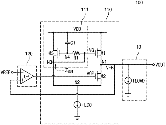
1. A low dropout (LDO) regulator, comprising:
a first resistor;
a first transistor including a gate terminal connected with a first end of the first resistor, a source terminal connected with a power supply voltage terminal, and a drain terminal connected with a first node;
an operational amplifier including input terminals respectively connected with a reference voltage and the first node, and an output terminal;
a second transistor including a gate terminal connected with the output terminal of the operational amplifier, a source terminal connected with the first node, and a drain terminal connected with a second node;
a third transistor including a gate terminal connected with a second end of the first resistor, a source terminal connected with the power supply voltage terminal, and a drain terminal connected with a third node; and
a current source connected between the second node and a ground voltage terminal.
|