| CPC G05F 1/56 (2013.01) [H01L 27/092 (2013.01); H01L 27/1203 (2013.01); H01L 29/42376 (2013.01); H01L 29/7831 (2013.01); H01L 29/7838 (2013.01)] | 13 Claims |
|
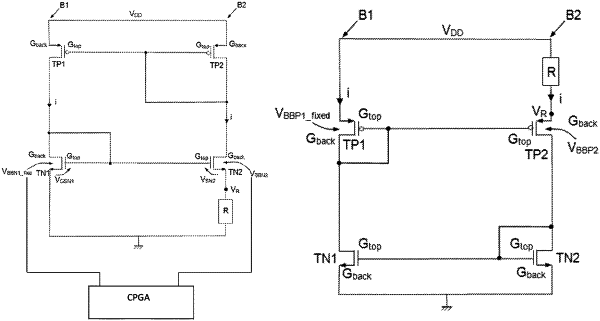
1. An electronic voltage divider circuit comprising at least two Fully Depleted Silicon on Insulator (FDSOI) transistors on insulating thin film (TP1, TP2) of a first type connected to a first supply potential and arranged in a current mirror structure and two FDSOI transistors on thin film (TN1, TN2) of a second type and an electrical load of non-zero impedance (R), the transistors each having a front-face main gate (Gtop) and a back-face control gate (Gback), a drain of a first transistor (TN1) of the second type being connected to the drain of a first transistor (TP1) of the first type, a drain of a second transistor (TN2) of the second type being connected to the drain of a second transistor (TP2) of the first type, the drain of the first transistor of the second type being connected to the front-face gate of this same transistor, the front-face gates of the first and second transistors of the second type being connected to one another, the source of the first transistor of the second type being connected to a second supply potential and said load of non-zero impedance being placed between the source of the second transistor of the second type and said second supply potential,
wherein the back-face gates of the first and second transistors of the second type (TN2) are connected to an external circuit (CPGA) applying a non-zero input voltage between these two back-face gates, such that the back-face gate of the first transistor of the second type is brought to a potential (VBBN1) lower than that (VBBN2) of the back-face gate of the second transistor of the second type if these two transistors are of nMOS type, and that the back-face gate of the first transistor of the second type is brought to a potential (VBBP1) greater than that (VBBP2) of the back-face gate of the second transistor of the second type if these two transistors are of pMOS type;
as a result of which the voltage across the terminals of said load (VRO) constitutes an output voltage equal to a fraction of the input voltage.
|