| CPC G05F 1/468 (2013.01) [H02M 3/158 (2013.01)] | 6 Claims |
|
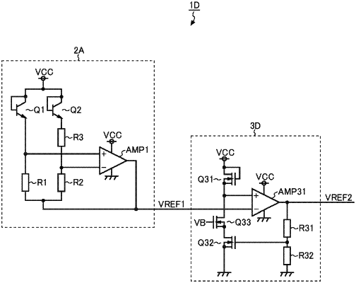
1. A reference voltage generation circuit, comprising:
a band gap reference circuit configured to generate a first reference voltage that depends on a band gap reference voltage and a supply voltage; and
a conversion circuit configured to convert the first reference voltage into a second reference voltage,
wherein:
the second reference voltage depends on the band gap reference voltage and a ground voltage,
the ground voltage is lower than the supply voltage,
the conversion circuit includes an amplifier,
an output terminal of the band gap reference circuit and a first input terminal of the amplifier are connected together with no resistive element therebetween, and
the conversion circuit further includes:
a first transistor between a first application terminal, to which the supply voltage is applied, and a second input terminal of the amplifier; and
a second transistor between the second input terminal of the amplifier and a second application terminal, to which the ground voltage is applied,
wherein:
a control terminal of the first transistor is connected to the first application terminal, and
the second reference voltage, or a division voltage of the second reference voltage, is fed to the control terminal of the second transistor.
|