US 11,940,737 B2
Method of fabricating reticle
Hsueh-Yi Chung, Hsinchu County (TW); Yung-Cheng Chen, Hsinchu County (TW); Fei-Gwo Tsai, Taipei (TW); Chi-Hung Liao, New Taipei (TW); Shih-Chi Fu, Hsinchu County (TW); Wei-Ti Hsu, Hsinchu County (TW); Jui-Ping Chuang, Hsinchu (TW); Tzong-Sheng Chang, Hsinchu County (TW); Kuei-Shun Chen, Hsinchu (TW); and Meng-Wei Chen, Taichung (TW)
Assigned to TAIWAN SEMICONDUCTOR MANUFACTURING CO., LTD., Hsinchu (TW)
Filed by TAIWAN SEMICONDUCTOR MANUFACTURING CO., LTD., Hsinchu (TW)
Filed on May 7, 2021, as Appl. No. 17/315,087.
Application 16/740,256 is a division of application No. 16/127,017, filed on Sep. 10, 2018, granted, now 10,534,272, issued on Jan. 14, 2020.
Application 17/315,087 is a continuation of application No. 16/740,256, filed on Jan. 10, 2020, granted, now 11,003,091.
Application 16/127,017 is a continuation of application No. 14/706,871, filed on May 7, 2015, granted, now 10,073,354, issued on Sep. 11, 2018.
Claims priority of provisional application 62/072,250, filed on Oct. 29, 2014.
Prior Publication US 2021/0263425 A1, Aug. 26, 2021
This patent is subject to a terminal disclaimer.
Int. Cl. G03F 7/20 (2006.01); G03F 1/50 (2012.01); G03F 1/68 (2012.01); G03F 1/70 (2012.01); G03F 1/78 (2012.01); G03F 7/00 (2006.01); H01L 21/66 (2006.01)
CPC G03F 7/70433 (2013.01) [G03F 1/50 (2013.01); G03F 1/68 (2013.01); G03F 1/70 (2013.01); G03F 1/78 (2013.01); G03F 7/20 (2013.01); G03F 7/70141 (2013.01); G03F 7/70158 (2013.01); G03F 7/70716 (2013.01); H01L 22/30 (2013.01)] 20 Claims
OG exemplary drawing
 
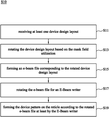
1. A method, comprising:
receiving a device design layout;
rotating the device design layout in a first direction;
providing a scribe line design layout to surround the rotated device design layout;
rotating the scribe line design layout in the first direction;
after rotating the scribe line design layout in the first direction, performing an optical proximity correction (OPC) process on the unrotated device design layout and the rotated scribe line design layout; and
forming a reticle comprising the device design layout and the scribe line design layout after performing the OPC process.