| CPC G03B 21/604 (2013.01) [H04N 9/3194 (2013.01); G02F 1/133365 (2013.01); G02F 1/133528 (2013.01)] | 15 Claims |
|
1. A projection display device, comprising:
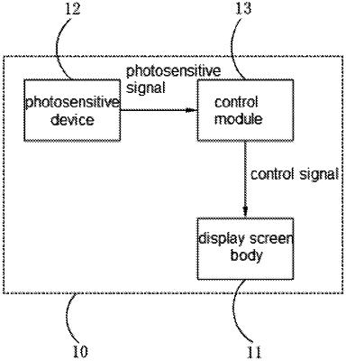
an image displaying part comprising a display screen body and a photosensitive device configured to sense a projection light beam projected on the projection display device, wherein the photosensitive device outputs a photosensitive signal when sensing the projection light beam;
a transparent glass part connected to the image displaying part; and
a control module electrically connected to the display screen body and the photosensitive device to receive the photosensitive signal, and to determine a projection position of the projection light beam on the projection display device and control a section of the display screen body corresponding to the projection position to be converted from a transparent state to an opaque state according to the photosensitive signal;
wherein the display screen body comprises a first transparent substrate and a second transparent substrate disposed opposite to the first transparent substrate, a switch device layer and a first electrode are stacked on one side of the first transparent substrate adjacent to the second transparent substrate in sequence, a second electrode is disposed on one side of the second transparent substrate adjacent to the first transparent substrate, and a liquid crystal layer is disposed between the first electrode and the second electrode;
wherein the switch device layer comprises a switch device electrically connected to the first electrode, and the control module is electrically connected to the switch device and controls the switch device to be turned on when receiving the photosensitive signal; wherein the transparent glass part is connected to the first transparent substrate, the second transparent substrate, the first electrode, and the second electrode, but not directly connected to the liquid crystal layer.
|