| CPC G02F 1/1368 (2013.01) [G02F 1/136227 (2013.01)] | 6 Claims |
|
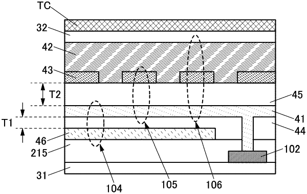
1. A display device comprising:
a pixel comprising a first transistor comprising a semiconductor layer, and a second transistor;
a first insulating layer over a channel formation region of the first transistor;
a first conductive layer over the first insulating layer;
a second insulating layer over the first transistor, the second transistor, the first insulating layer, and the first conductive layer;
a pixel electrode over the second insulating layer;
a third insulating layer over the pixel electrode;
a common electrode over the third insulating layer; and
a liquid crystal layer over the common electrode,
wherein the common electrode comprises a region overlapping with the first conductive layer with the pixel electrode therebetween,
wherein the pixel electrode is electrically connected to the first transistor,
wherein the first conductive layer is electrically connected to the second transistor,
wherein each of the first conductive layer, the pixel electrode, and the common electrode is configured to transmit visible light, and
wherein the semiconductor layer comprises a different material from the first conductive layer, or the first conductive layer comprises a different material from the semiconductor layer.
|