| CPC G02F 1/1368 (2013.01) [H01L 29/0847 (2013.01); H01L 29/1033 (2013.01); H01L 29/24 (2013.01); H01L 29/66969 (2013.01); H01L 29/786 (2013.01); H01L 29/78633 (2013.01); H01L 29/7869 (2013.01); H10K 50/115 (2023.02); G06F 3/0412 (2013.01); G06F 3/0443 (2019.05); G06F 3/0446 (2019.05)] | 6 Claims |
|
1. A semiconductor device comprising:
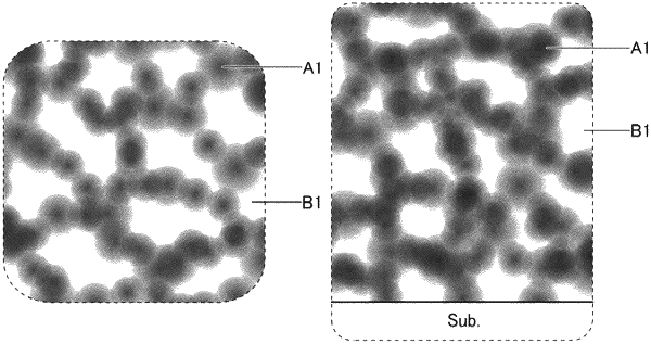
an oxide semiconductor film over a substrate, the oxide semiconductor film comprising a first region comprising In and Zn and a second region comprising In and Zn,
wherein in a cross-sectional view, the first region and the second region are arranged in a same plane along a direction parallel to a top surface of the substrate,
wherein the first region comprises a plurality of first clusters,
wherein the second region comprises a plurality of second clusters,
wherein in a cross-sectional view and a plane view of the oxide semiconductor film, the plurality of first clusters are directly connected to each other in three dimensions,
wherein in a cross-sectional view and a plane view of the oxide semiconductor film, the plurality of second clusters are partly connected to each other,
wherein the plurality of first clusters are sandwiched by the plurality of second clusters in the three dimensions, and
wherein an In concentration in the first region is 2 or more times and 10 or less times an In concentration in the second region.
|