| CPC G02F 1/1368 (2013.01) [G02F 1/136295 (2021.01); G02F 1/13718 (2013.01)] | 18 Claims |
|
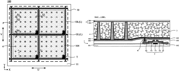
1. A writing panel, comprising:
an array substrate, the array substrate including a base and a pixel driving circuit layer disposed on the base, the pixel driving circuit layer including a plurality of thin film transistors and a plurality of signal lines;
a flexible substrate disposed opposite to the array substrate;
a liquid crystal layer disposed between the array substrate and the flexible substrate; and
a plurality of spacers each in a shape of a column disposed on a surface of the array substrate proximate to the liquid crystal layer, an orthographic projection of each spacer on the base being non-overlapping with orthographic projections of the plurality of thin film transistors and the plurality of signal lines on the base,
wherein the writing panel has a plurality of pixel regions;
each pixel region is provided with some of the plurality of spacers therein, and the some of the plurality of spacers are arranged in an array; and
a row direction of the array in which the some of the plurality of spacers are arranged is a first direction, and a column direction of the array in which the some of the plurality of spacers are arranged is a second direction;
in a pixel region of the pixel regions, a distance between two spacers adjacent to each other in the first direction is approximately equal to a distance between two spacers adjacent to each other in the second direction; and
a distance between two nearest spacers that are respectively located in two pixel regions adjacent to each other in the first direction is approximately equal to a distance between two nearest spacers that are respectively located in two pixel regions adjacent to each other in the second direction.
|