| CPC G02F 1/136286 (2013.01) [G02F 1/13456 (2021.01); G02F 1/13458 (2013.01); G02F 1/136227 (2013.01); G02F 1/1368 (2013.01)] | 18 Claims |
|
1. An array substrate for a liquid crystal display panel, comprising a display area and a non-display area at a periphery of the display area, wherein
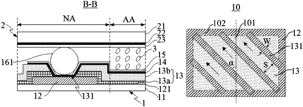
the array substrate is provided with a plurality of conductive bonding pads distributed at intervals in the non-display area, in which the conductive bonding pad comprises a first metal layer, an insulating layer and a conductive layer sequentially formed on a first base substrate, in which the first metal layer is in the same layer with and is electrically connected to a first common electrode in the display area, and the insulating layer is provided with a plurality of vias to electrically connect the conductive layer to the first common electrode, in which the via is provided in a slit shape and is disposed at a predetermined angle from a first direction in which the non-display area surrounds the display area.
|