| CPC G02F 1/136277 (2013.01) [G02F 1/133302 (2021.01); G02F 1/133351 (2013.01); G02F 1/1339 (2013.01); G02F 1/1341 (2013.01); H01L 21/76898 (2013.01); H01L 21/78 (2013.01)] | 17 Claims |
|
1. A preparation method of a liquid crystal on silicon (LCoS) panel, comprising:
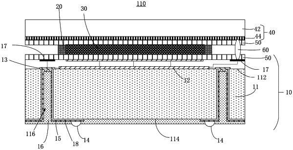
providing a wafer substrate, wherein the wafer substrate comprises a silicon substrate and a plurality of die areas defined by a plurality of intersecting dividing lines, the silicon substrate comprises a first surface and a second surface opposite to the first surface, each of the plurality of die areas comprises an active circuit on the first surface, and the active circuit comprises a pixel circuit area and a peripheral circuit area;
performing wafer level packaging by:
manufacturing a plurality of vias extending through the first surface and the second surface in each of the plurality of die areas of the wafer substrate; and
manufacturing a plurality of conductive interfaces on the second surface, wherein each of the plurality of conductive interfaces is arranged to correspond to one of the plurality of vias, and each of the plurality of conductive interfaces is electrically connected to the active circuit of one of the plurality of die areas where the conductive interface is located by a corresponding one of the plurality of vias;
performing liquid crystal packaging by:
forming a seal on the first surface in each of the plurality of die areas of the wafer substrate, wherein the seal at least surrounds the pixel circuit area of the active circuit, and defines a liquid crystal space of one of the plurality of die areas where the seal is located;
injecting liquid crystal into the liquid crystal space of the wafer substrate;
providing a glass substrate comprising a transparent conductive layer, and
forming a plurality of enclosed spaces filled with the liquid crystal by coupling a surface of the glass substrate with the transparent conductive layer and the wafer substrate by the seal; and
cutting the wafer substrate along the plurality of dividing lines, cutting the glass substrate, and further obtaining a plurality of LCoS panels, wherein each of the plurality of LCoS panels is provided with a corresponding one of the plurality of enclosed spaces, an LCoS module is obtained when one of the plurality of LCoS panels is electrically connected to an external circuit substrate, and the active circuit is electrically connected to the external circuit substrate by the plurality of vias and the plurality of conductive interfaces in sequence; and during the wafer level packaging, projections of the plurality of vias on the wafer substrate surround and keep away from the pixel circuit area in each of the plurality of die areas.
|