| CPC G02F 1/136213 (2013.01) [G02F 1/13624 (2013.01); G02F 1/136286 (2013.01); G02F 1/1368 (2013.01); G09G 3/3648 (2013.01); G09G 3/3659 (2013.01); G02F 1/134345 (2021.01); G02F 1/136227 (2013.01); G02F 1/136295 (2021.01); G09G 3/2022 (2013.01); G09G 3/3233 (2013.01); G09G 2300/0443 (2013.01); G09G 2300/0447 (2013.01); G09G 2300/0809 (2013.01); G09G 2300/0842 (2013.01); G09G 2300/0852 (2013.01); G09G 2310/0262 (2013.01); G09G 2320/0252 (2013.01); G09G 2320/0261 (2013.01); G09G 2320/028 (2013.01); G09G 2320/10 (2013.01); G09G 2320/106 (2013.01); G09G 2330/021 (2013.01); G09G 2340/0435 (2013.01); G09G 2340/16 (2013.01); H01L 27/12 (2013.01)] | 2 Claims |
|
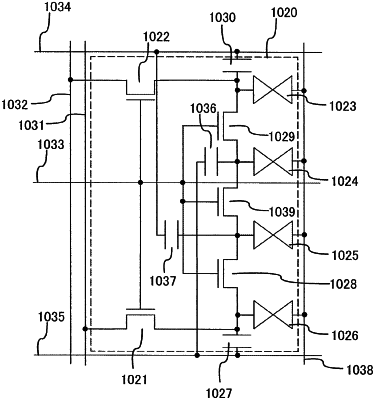
1. A liquid crystal display device comprising a first pixel,
the first pixel comprising:
a signal line;
a scan line;
a first transistor, a second transistor, and a third transistor each comprising a gate, a first terminal, and a second terminal;
a first capacitor, a second capacitor, and a third capacitor each comprising a first terminal and a second terminal; and
a first liquid crystal element and a second liquid crystal element each comprising a first electrode and a second electrode,
wherein the gate of the first transistor, the gate of the second transistor, and the gate of the third transistor are electrically connected to the scan line,
wherein the first terminal of the first transistor is electrically connected to the first electrode of the first liquid crystal element and to the first terminal of the first capacitor,
wherein the first terminal of the second transistor is electrically connected to the first electrode of the second liquid crystal element and to the first terminal of the second capacitor,
wherein the first terminal of the third transistor is electrically connected to the first terminal of the third capacitor,
wherein the second terminal of the third transistor is electrically connected to the first terminal of the first capacitor,
wherein the second terminal of the first transistor and the second terminal of the second transistor are electrically connected to the signal line,
wherein the second terminal of the first capacitor is electrically connected to a first capacitor line,
wherein the second terminal of the second capacitor is electrically connected to a second capacitor line,
wherein the scan line is arranged between the first electrode of the first liquid crystal element and the first electrode of the second liquid crystal element.
|