| CPC G02F 1/13394 (2013.01) [G02F 1/13415 (2021.01); G02F 2202/28 (2013.01)] | 15 Claims |
|
1. A light modulation device, comprising a first glass substrate, a bonding layer and a light modulation panel, wherein the light modulation panel comprises:
a first substrate and a second substrate arranged in align with each other;
a liquid crystal filled between the first substrate and the second substrate; and
spacer structures located between the first substrate and the second substrate and the spacer structures are configured to maintain a cell gap of the liquid crystal;
wherein the spacer structure comprises a first post spacer and a second post spacer arranged in layer configuration, the first post spacer is arranged on a side of the first substrate close to the second substrate, the second post spacer is arranged on a side of the second substrate close to the first substrate, a first surface of the first post spacer and a second surface of the second post spacer face and contact each other;
the bonding layer is configured to bond the first glass substrate and a first substrate or a second substrate of the light modulation panel; and
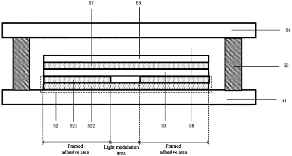
the light modulation panel further comprises a light modulation area and a framed adhesive area located in a periphery of the light modulation area, the bonding layer comprises a first adhesive film layer, the first adhesive film layer is an annular adhesive tape, an orthographic projection of the annular adhesive tape on the light modulation panel is located in the framed adhesive area, the annular adhesive tape is formed with notches, and the notches are configured to communicate an internal area surrounded by the annular adhesive tape with an external area of the annular adhesive tape.
|