| CPC G02F 1/133611 (2013.01) [C08G 77/12 (2013.01); G02F 1/133603 (2013.01); G02F 1/133605 (2013.01); G02F 1/133608 (2013.01); G02F 2201/50 (2013.01); G02F 2202/10 (2013.01)] | 21 Claims |
|
1. A display device comprising:
a plurality of light sources;
a resin layer disposed to cover the plurality of light sources;
a reflective plate that is disposed on a printed circuit board and has a plurality of through-holes respectively penetrated by the plurality of light sources; and
a display panel disposed on the resin layer and including a display area and a non- display area,
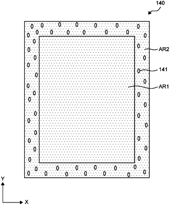
wherein the resin layer comprises:
a first region configured to overlap the display area; and
a second region configured to overlap the non-display area, and
wherein a plurality of fine holes are provided in at least a part of the second region,
wherein a solder resist is disposed on the printed circuit board on which the plurality of light sources are disposed, the reflective plate covers the solder resist, and the reflective plate and the solder resist are respectively patterned to overlap each other, and
wherein a porosity of the second region is larger than a porosity of the first region, and
wherein a moisture vapor transmittance rate of the second region is larger than a moisture vapor transmittance rate of the first region.
|