| CPC G02F 1/133553 (2013.01) [G02F 1/133742 (2021.01); G02F 1/134309 (2013.01); G02F 1/136227 (2013.01); G02F 2203/09 (2013.01)] | 9 Claims |
|
1. A liquid crystal display device comprising:
first and second substrates;
a liquid crystal layer interposed between the first and second substrates and set in vertical alignment (VA) when no electric field is applied;
a switching element provided on the first substrate;
a connection electrode provided on the first substrate, connected to the switching element, and extending in a first direction;
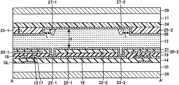
a first reflection film provided above the switching element with an insulating film therebetween, and configured to reflect light;
a first pixel electrode provided above the first reflection film with an insulating film therebetween, overlapping the first reflection film in planar view, and formed of a transparent electrode;
a second pixel electrode located adjacent to the first pixel electrode in the first direction, and formed of a transparent electrode;
first and second contacts which respectively connect the first and second pixel electrodes to the connection electrode;
a first thickness adjusting layer provided on the second substrate and overlapping the first reflection film in planar view;
a common electrode provided on the second substrate and the first thickness adjusting layer; and
first and second protrusions provided on the common electrode and respectively corresponding to the first and second pixel electrodes,
wherein a thickness of the liquid crystal layer in a reflection area where the first reflection film is disposed is smaller than a thickness of the liquid crystal layer in a transmission area where no reflection film is disposed by a thickness of the first thickness adjusting layer, and
the first protrusion is located closer to the first thickness adjusting layer than a center of the first pixel electrode is in the first direction.
|