| CPC G02F 1/133512 (2013.01) [G02F 1/1334 (2013.01); G02F 1/133553 (2013.01); G02F 1/133615 (2013.01); G02F 1/136209 (2013.01); G02F 1/136286 (2013.01); G02F 1/133345 (2013.01); G02F 1/133365 (2013.01); G02F 1/1337 (2013.01); G02F 1/134309 (2013.01); G02F 1/13452 (2013.01); G02F 2201/121 (2013.01); G02F 2201/123 (2013.01)] | 4 Claims |
|
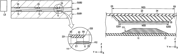
1. A display device, comprising:
a first substrate;
a scanning line including a first side and a second side on the first substrate;
a second substrate opposed to the first substrate;
a light-shielding layer including a third side and a fourth side, and overlapping the scanning line on the second substrate;
a liquid crystal layer held between the first substrate and the second substrate, and which includes a polymer and liquid crystal molecules; and
a light-emitting element arranged along a side of the second substrate, wherein
the first side of the scanning line is closer to the light-emitting element than the second side of the scanning line,
the third side of the light-shielding layer is located closer to the light-emitting element than the first side of the scanning line, and
the second side of the scanning line overlaps the fourth side of the light-shielding layer.
|