| CPC G02F 1/1323 (2013.01) [G02B 6/0051 (2013.01); G02F 1/1334 (2013.01); G02F 1/133512 (2013.01); G02F 1/134309 (2013.01); G02F 1/13476 (2013.01); G02F 2201/50 (2013.01)] | 19 Claims |
|
1. A display panel, comprising:
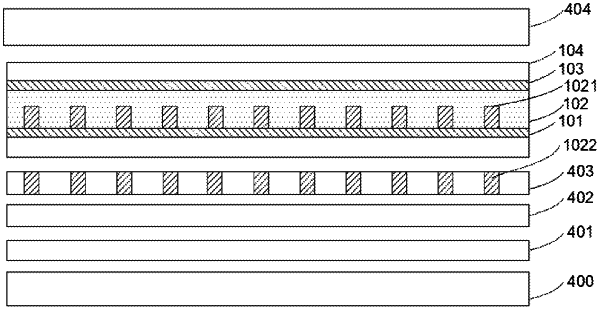
a first substrate;
a first electrode layer disposed on the first substrate;
a second electrode layer disposed on a liquid crystal layer;
a second substrate disposed on the second electrode layer; and
a protective layer disposed on the second substrate,
wherein the display panel further comprises a light control layer, the light control layer is disposed between the first electrode layer and the second electrode layer, the light control layer comprises a first liquid crystal and light blocking layers, and the light blocking layers are disposed on a side of the light control layer close to the first electrode layer; and when no voltage is applied to the light control layer, the first liquid crystal is configured as an atomized liquid crystal for scattering light, and when a voltage is applied to the light control layer, the first liquid crystal is configured as a transparent liquid crystal, and the first liquid crystal comprises a polymer network liquid crystal material,
wherein the display panel further comprises:
a light guide plate;
a diffusion layer disposed on the light guide plate;
at least one anti-reflection layer disposed on the diffusion layer, wherein the second substrate is disposed on the anti-reflection layer,
wherein a side of the diffusion layer away from the anti-reflection layer is arranged in a zigzag structure, and a side of the light guide plate away from the anti-reflection layer is arranged in a convex-concave shape structure.
|