| CPC G02F 1/025 (2013.01) [G02F 2201/063 (2013.01); G02F 2202/105 (2013.01)] | 20 Claims |
|
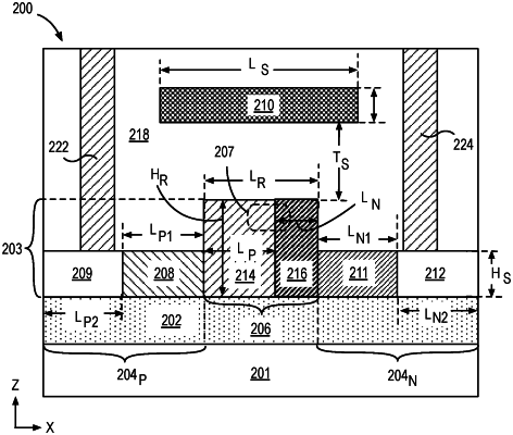
1. An optical modulator apparatus, comprising:
a first dielectric layer over a substrate;
a rib waveguide comprising a PN junction on the first dielectric layer, the PN junction of the rib waveguide comprising a P-doped region adjacent an N-doped region;
a first slab region adjacent to the P-doped region and a second slab region adjacent to the N-doped region;
a second dielectric layer over the rib waveguide; and
a stressor layer comprising a metal, wherein the second dielectric layer is between the stressor layer and the PN junction, and wherein the stressor layer extends laterally above the first slab region and the second slab region.
|